Co-Packaged Optics Testing
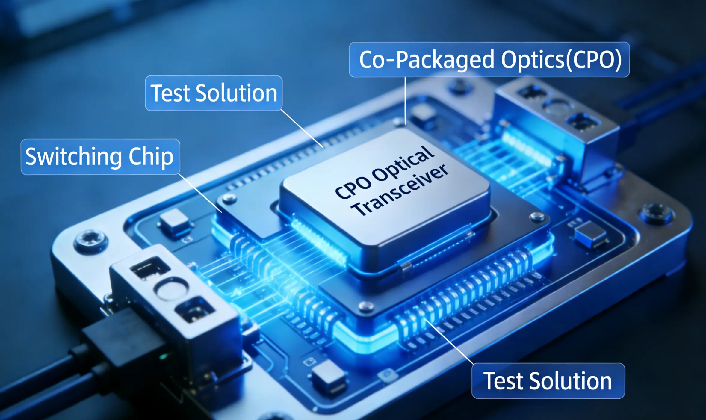
For Co-Packaged Optics (CPO), we offer customized test solutions to meet next-gen data center interconnect demands. CPO integrates optical transceivers with switching chips, shortening signal paths, reducing power consumption, and increasing bandwidth density—a key future trend. With flexible test architecture and deep technical expertise, we enable efficient, reliable optoelectronic co-verification from R&D to mass production.
For CPO testing, we collaborate with customers to develop dedicated wafer-level test solutions addressing high-density integration, thermal complexity, and high channel counts. Our multi-channel parallel test systems balance optical coupling precision and throughput, supporting optoelectronic parameter evaluation from R&D to production. We provide flexible, scalable solutions for silicon photonic engines, CW lasers, and switching chips, accelerating CPO products from design to market.
Co-Packaged Optics
Near-Packaged Optics
Note: NPO serves as a transitional solution between CPO and traditional pluggable modules, offering a balanced approach between performance and manufacturability for near-term data center upgrades

Supports multi-channel parallel testing, significantly reducing single-chip test time and meeting high-throughput production demands
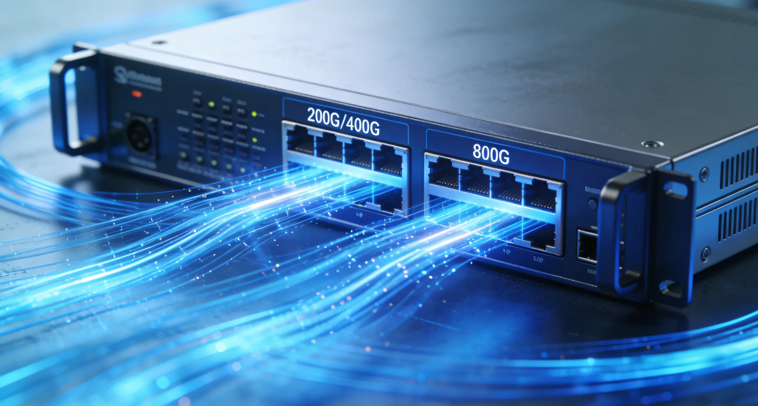
Supports high-speed optical signal testing from 200G to 3.2T, covering the data rates required for next-generation data center interconnects

Provides comprehensive eye diagram analysis for signal quality and link integrity, enabling rapid diagnostics

Integrated fully automated probe station, comprising hexapod positioning stage, fiber array unit (FAU), microscope, and other essential components.
Common questions about silicon photonics testing
Our system supports 4", 6", 8" and 12" (300mm) wafers, meeting various needs from R&D to production.
Edge-coupling is suitable for high coupling efficiency scenarios, while grating coupler is better for mass production.
NPO as a transitional solution has relatively lower packaging complexity and technical difficulty, making it easier to implement; CPO represents a longer-term technology direction. We provide professional recommendations based on your product positioning and application scenarios.
Our system achieves sub-micron to nanometer alignment precision, fully meeting silicon photonic device testing requirements.
Yes, we have a testing laboratory at Singapore Science Park, providing wafer testing services and system demonstrations.
Yes, Navigo provides rich API interfaces, supporting customer customization and secondary development.
Standard products typically take 6-8 months, customized products depend on specific requirements.