Silicon photonics wafer testing faces many challenges, mainly in technical complexity, test speed, precision, and cost
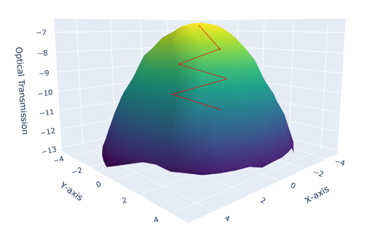
High Precision: Silicon photonics testing needs sub-micron or nanometer alignment precision.
High Speed: Fast automated testing needed for large-scale silicon photonics production.
Learn More →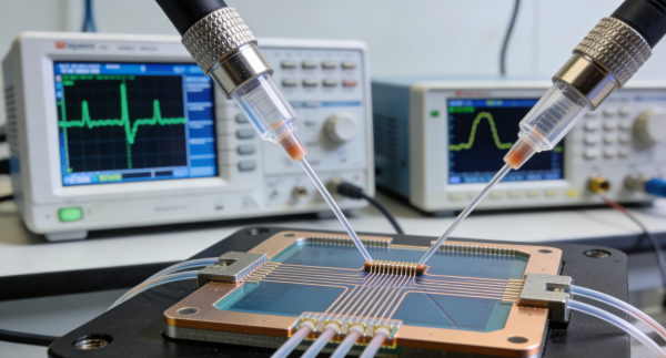
Optical Alignment: Micron misalignment causes inaccurate test results for photonic devices.
Multi-Parameter Testing: Silicon photonics testing includes IL, PDL, I-V, bandwidth, and eye diagrams.
Learn More →
Diversity: Silicon photonics devices (modulators, detectors, etc.) have different test methods.
Integration: Increased integration demands testing of more complex optoelectronic functions.
Learn More →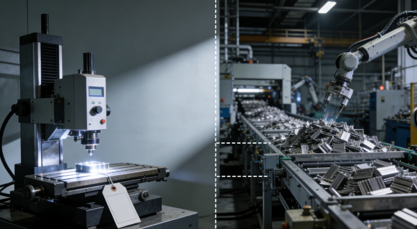
Equipment Cost: High-precision test equipment is expensive; balance performance and cost.
Test Efficiency: Balancing efficiency and low cost in mass production challenges manufacturers.
Learn More →
Large Amounts of Data:PIC testing generates large data volumes, requiring efficient processing and analysis to quickly identify and address issues.
Data Accuracy: Ensuring data accuracy and consistency to guarantee the reliability of test results.
Learn More →
Automation: Increasing the level of automation in the testing process to reduce human error and improve testing efficiency.
Flexibility: Testing systems must be flexible to adapt to different silicon photonic devices and testing requirements.
Learn More →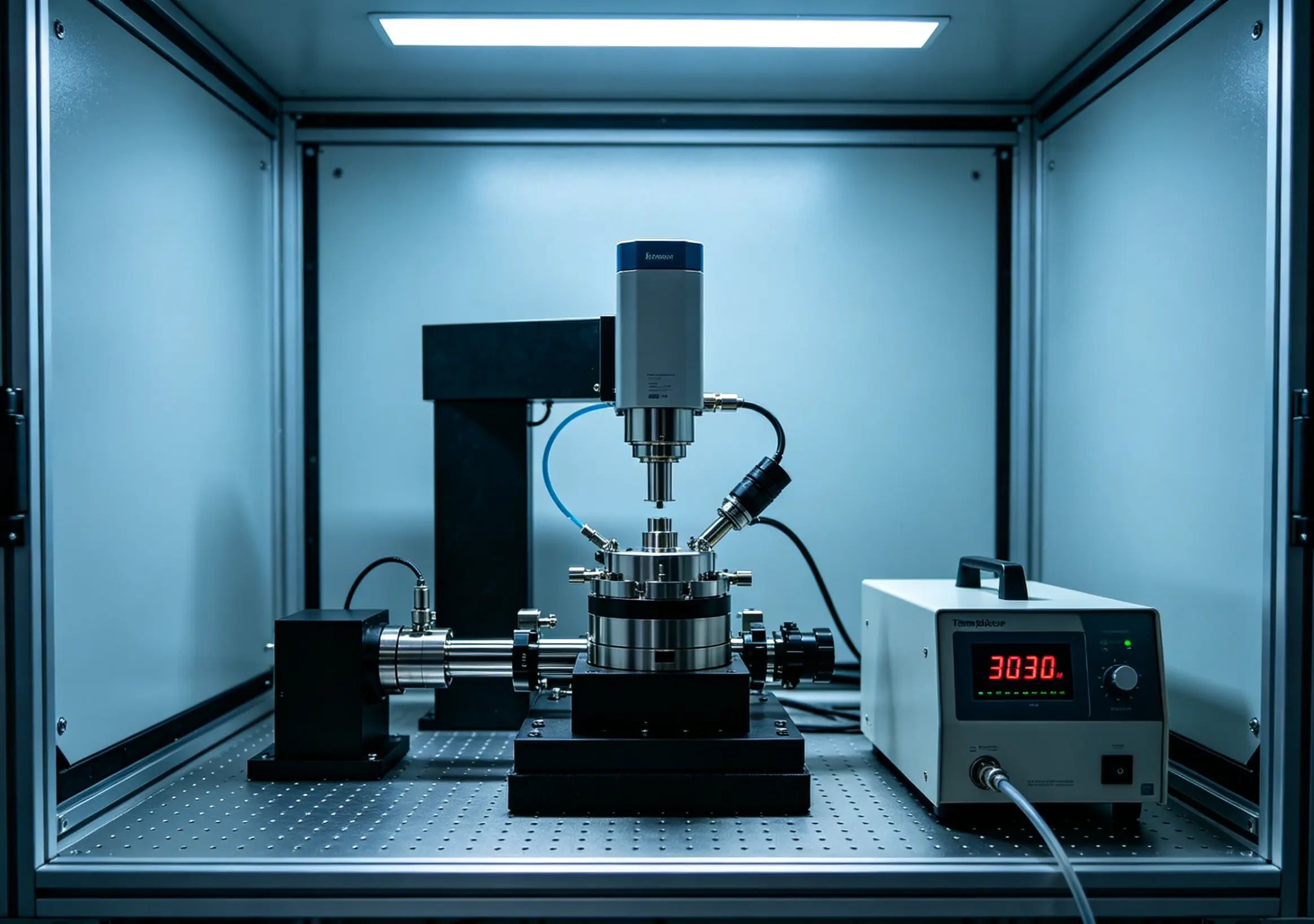
Environmental Stability: The testing environment needs to remain highly stable to avoid external interference affecting the test results, such as vibration and temperature fluctuations.
Learn More →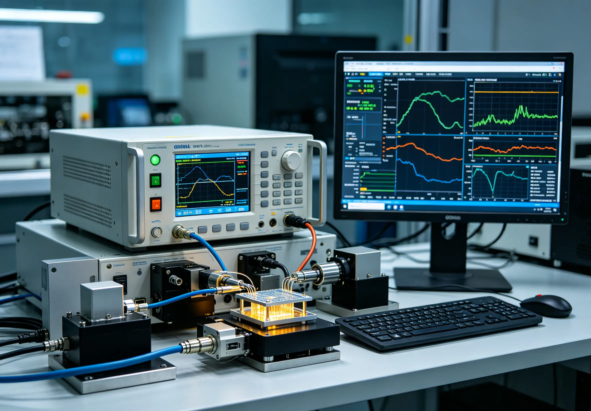
Addressing these challenges requires advanced testing equipment, automation software, and system integration experience. Sunyu Photonics provides high-precision, high-speed automation solutions to improve PIC testing efficiency and quality.
Learn More →Our wafer-level automation test solutions, controlled by Navigo software, integrate high-precision probe stations and various optoelectronic test instruments
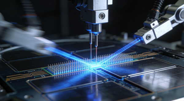
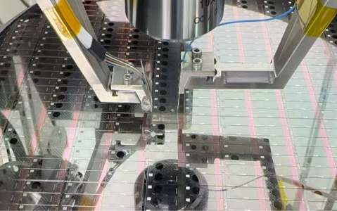
Our automation test system is designed for silicon photonics chips, achieving high-precision, high-efficiency wafer-level testing. Supports comprehensive testing from R&D to production.
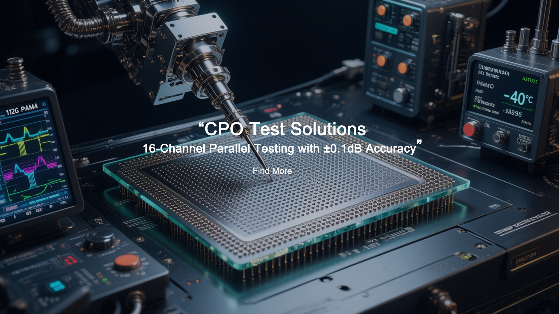
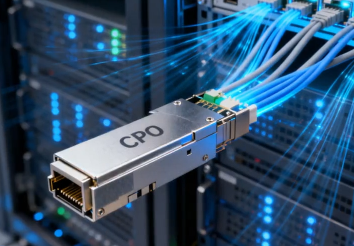
For Co-Packaged Optics (CPO) technology, we provide specialized testing solutions to meet the needs of next-generation data center interconnects.
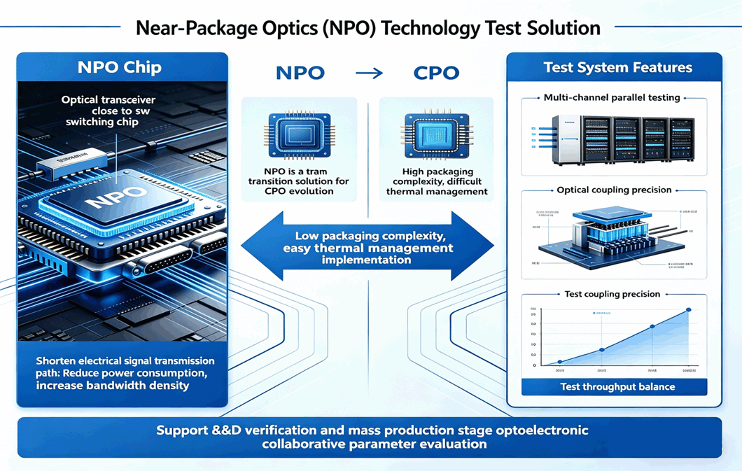
For Near-Packaged Optics (NPO) technology, we provide specialized test solutions to meet the needs of next-generation data center interconnect.
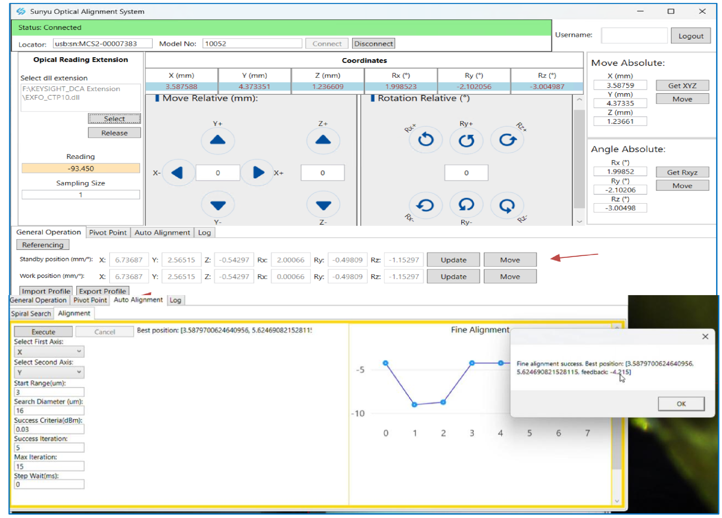
Our proprietary PIC test system software Navigo is the core of high-precision, high-efficiency automated PIC testing. Provides intuitive interface and powerful data processing capabilities.
We have established an advanced silicon photonics testing lab in Singapore Science Park
Providing wafer testing services for local customers and clients worldwide.
Learn More →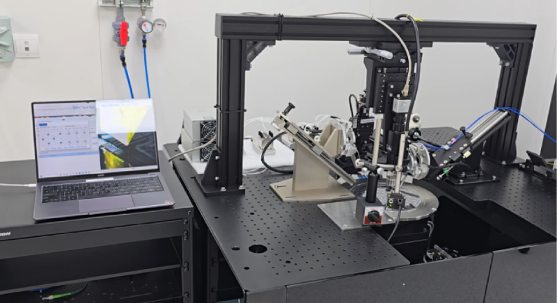
Providing system demonstrations to help customers understand our solutions.
Learn More →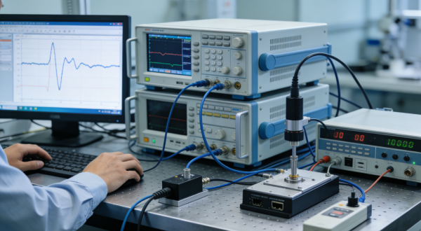
Customized test system development and integration services.
Learn More →


We have established long-term partnerships with many industry-leading companies


Contact our expert team today for customized solution recommendations.
Contact Us