Driving innovation at the forefront of integrated photonics technology.

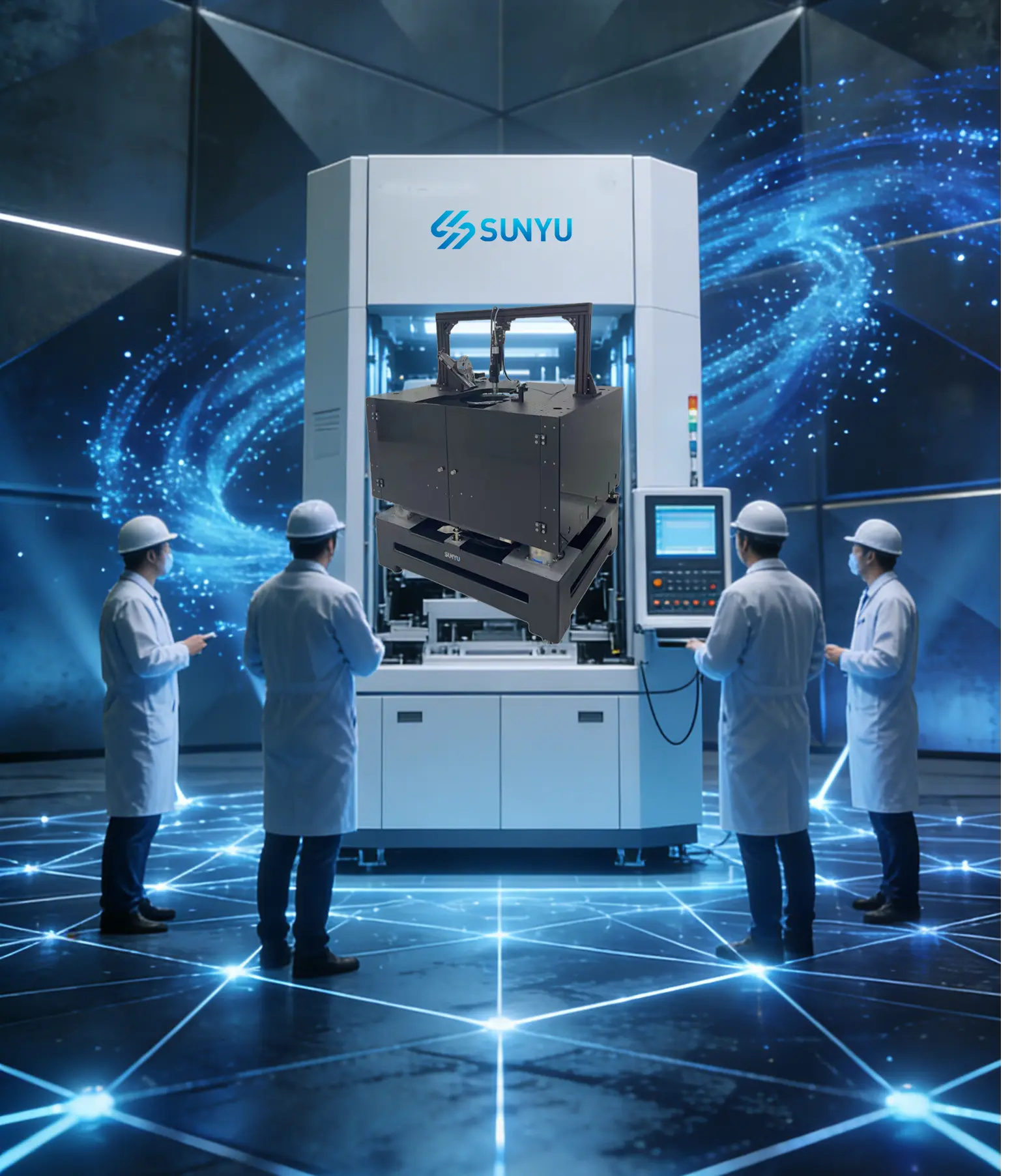
Sunyu is at the forefront of integrated photonics technology, developing and providing advanced wafer-level test automation systems to drive innovation in this field. We are committed to providing customers with high-precision, high-efficiency testing solutions for all stages from R&D to production.
As a total test system solution provider, Sunyu has more than ten years of expertise in photonic integrated circuit testing, industrial automation, high-precision motion control, software development, and wafer-level test system integration and customization.
Witness Our Growth and Progress
Sunyu Photonics Technology Co., Ltd. established
Specializing in silicon photonics automated testing technology development
Established an advanced silicon photonics chip automated testing lab in Singapore, equipped with fully automatic wafer probe stations, optical and electrical testing instruments, and a 10k-class cleanroom.
Successfully launched the first self-developed fully automatic wafer probe station prototype
Completed delivery of the first PIC wafer-level test system, gaining customer recognition
Four Reasons to Choose Us
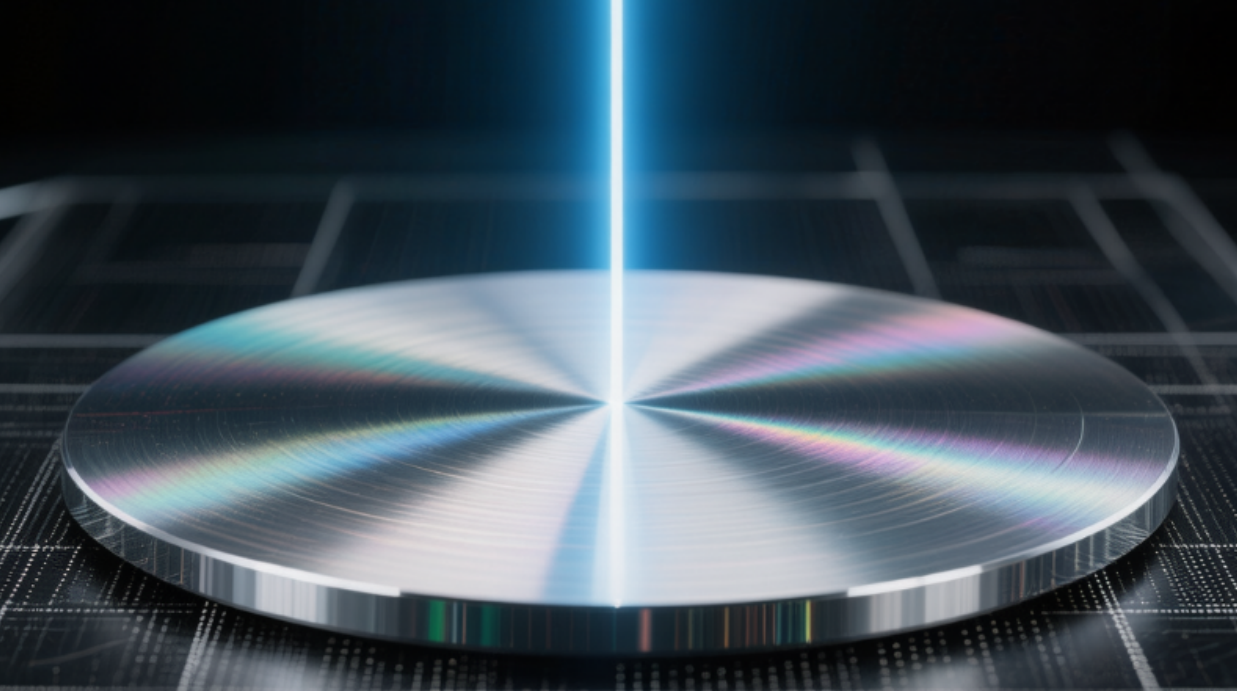
Alignment precision reaches sub-micron or nanometer level

Fully automated test process improves efficiency
Customized test system development

From Singapore hub, we deliver efficient pro-service worldwide.
We have comprehensive technical expertise and project experience
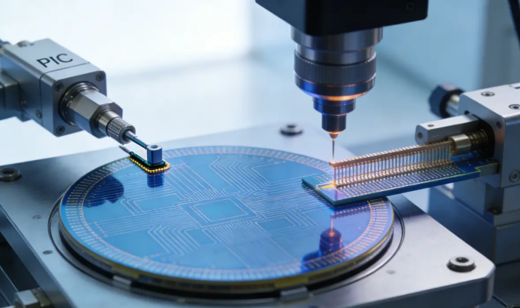
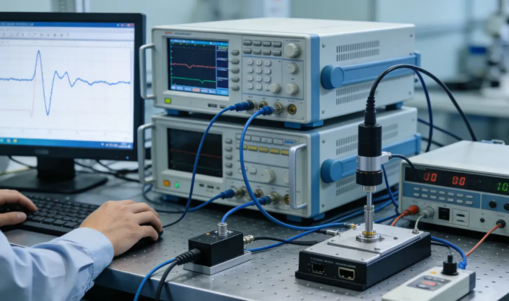
Specializing in PIC wafer-level testing, providing edge-coupling and grating coupler testing solutions

Complete automated test solutions, including loading, testing, and sorting processes
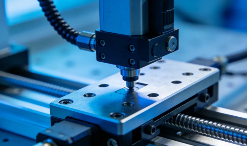
Sub-micron motion control platform ensures test accuracy and repeatability
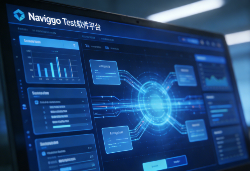
Navigo test software platform provides intuitive interface and powerful data processing